

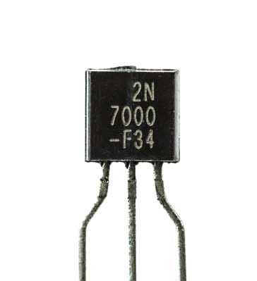
MOSFET – Metal Oxide Semiconductor Field Effect Transistor
The MOSFET or metal oxide semiconductor field effect transistor, is a form of FET that offers an exceedingly high input impedance.
The gate input has an oxide layer insulating it from the channel and as a result its input resistance is very many MΩ.
The MOSFET has a number of different characteristics compared to the junction FET, and as a result it can be used in a number of different areas and it is able to provide excellent performance.
One particular area where MOSFET technology is used is within CMOS logic integrated circuits. The extraordinarily high input impedance means that these circuits are able to consume very low power levels and this means that high levels of integration can be achieved.
MOSFET development
The concept of the MOSFET has been known for many years but they only became important in mid to late 1960s.
One of the major problems experienced with the early development of MOSFETs was associated in developing the insulating oxide layers. The problems were only overcome as the semiconductor materials and processing technology improved. As a result, in the late 1960s MOSFET technology became more widespread.
Now MOSFET technology is one of the most widely used semiconductor techniques, having become one of the principle elements in integrated circuit technology.
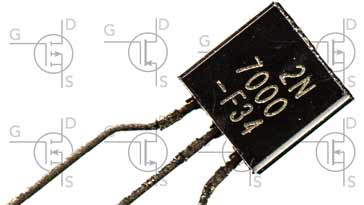
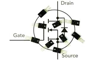
MOSFET circuit symbol
There is a variety of different circuit symbols used for MOSFETs. In view of the different variety of standards used, along with the different types of MOSFET, a host of different MOSFET circuit symbols can be seen.

MOSFET circuit symbol notes:
- The circuit symbol for the basic MOSFET (shown left most) indicates that the device has a bulk substrate – this is indicated by the arrow on the central area of the substrate.
- The MOSFET circuit symbols shown in the centre and marked “enhancement no bulk semi” are both valid and used equally frequently. They indicate an enhancement MOSFET that has no bulk semiconductor.
- Depletion mode MOSFETs are generally indicated as shown on the right most section.
MOSFET circuit symbols for both P-channel and N-channel types are shwn. The drain is shown at the top as this is generally as they are seen on circuit diagrams.
MOSFET key parameters
Before looking at the operation of the MOSFET, it is worth summarising a few of the key features associated with MOSFET technology.
| KEY MOSFET FEATURES | |
|---|---|
| FEATURE | DETAILS |
| Gate construction | The gate is physically insulated from the channel by an oxide layer. Voltages applied to the gate control the conductivity of the channel as a result of the electric field induced capacitively across the insulating dielectric layer. |
| N / P channel | Both N-channel and P-channel variants are available |
| Enhancement / depletion | Both enhancement and depletion types are available. As the name suggests the depletion mode MOSFET acts by depleting or removing the current carriers from the channel, whereas the enhancement type increases the number of carriers according to the gate voltage. |
MOSFETs may be characterised as N Channel and P-Channel. Each has different characteristics:
| COMPARISON OF THE KEY FEATURES OF N-CHANNEL AND P-CHANNEL MOSFETS | ||
|---|---|---|
| PARAMETER | N-CHANNEL | P-CHANNEL |
| Source / drain material | N-Type | P-Type |
| Channel material | P-Type | N-Type |
| Threshold voltage Vth | negative | doping dependent |
| Substrate material | P-Type | P-Type |
| Inversion layer carriers | Electrons | Holes |
MOSFET operation: how a MOSFET works
Like other forms of FET, the current flowing in the channel of the MOSFET is controlled by the voltage present on the gate. As such MOSFETs are widely used in applications such as switches and also amplifiers. They are also able to consume very low levels of current and as a result they are widely used in microprocessors, logic integrated circuits and the like. CMOS integrated circuits used MOSFET technology.
Note: In view of the structure of the MOSFET – its gate is insulated from the channel by a thin oxide layer and this means that it can be damaged by static if it is not handled in the correct way, or the circuit does not protect it adequately.
Also like other forms of FET, the MOSFET is available in depletion mode and enhancement mode variants. The enhancement mode is what may be termed normally OFF, i..e when the VGS gate source voltage is zero and requires a gate voltage to turn it on, whereas the other form, deletion mode devices are normally ON when VGS is zero.
There are basically three regions in which MOSFETs can operate:
- Cut-off region: In this region of the MOSFET is in a non-conducting state, i.e. turned OFF – channel current IDS = 0. The gate voltage VGS is less than the threshold voltage required for conduction.
- Linear region: In this linear region the channel is conducting and controlled by the gate voltage. For the MOSFET to be in this state the VGS must be greater than the threshold voltage and also the voltage across the channel, VDS must be greater than VGS.
- Saturation region: In this region the MOSFET is turned hard on. The voltage drop for a MOSFET is typically lower than that of a bipolar transistor and as a result power MOSFETs are widely used for switching large currents.
A power MOSFET in a TO220 packageSWITCHING FOR DIFFERENT TYPES OF MOSFETMOSFET TYPEVGS +VEVGS 0VGS -VEN-Channel EnhancementONOFFOFFN-Channel DepletionONONOFFP-Channel EnhancementOFFOFFONP-Channel DepletionOFFONON
MOSFET structure
As already implied the key factor of the MOSFET is the fact that the gate is insulated from the channel by a thin oxide layer. This forms one of the key elements of its structure.
For an N-channel device the current flow is carried by electrons and in the diagram below it can be seen that the drain and source are formed using N+ regions which provide good conductivity for these regions.
In some structures the N+ regions are formed using ion implantation after the gate area has been formed. In this way, they are self-aligned to the gate.
The gate to source and gate to drain overlap are required to ensure there is a continuous channel. Also the device is often symmetrical and therefore source and drain can be interchanged. On some higher power designs this may not always be the case.

It can be seen from the diagram that the substrate is the opposite type to the channel, i.e. P-type rather than N-type, etc. This is done to achieve source and drain isolation.
The oxide over the channel is normally grown thermally as this ensure good interfacing with the substrate and the most common gate material is polysilicon, although some metals and silicides can be used.
The depletion mode has a slightly different structure. For this a separate N-type channel is set up within the substrate.

P-channel FETs are not as widely used. The main reason for this is that the holes do not have as high a level of mobility as electrons, and therefore the performance is not as high. However they are often required for use in complementary circuits, and it is mainly for this reason that they are manufactured or incorporated into ICs.
MOSFETs are possibly the most widely used active device. As they appear in CMOS and other integrated circuit technologies where they enable very low power operation – a requirement for very large scale integration, otherwise power consumption would be far too high.
Not only are they used in IC technology, but they are also used as discrete components as well where they are able to offer very high input impedance levels and also low noise operation in oscillators, amplifiers and many other circuits.
Dual gate MOSFET
The dual gate MOSFET is a useful form of MOSFET which can provide some distinct advantages, especially in RF applications.
The dual gate MOSFET can be considered in the same light as the tetrode vacuum tube or thermionic valve. The introduction of the second control electrode considerably reduced the level of feedback capacitance between the input and output circuits of the device. In this way it is possible to make far more stable amplifiers.
Also the additional gate enables the dual gate MOSFET to be used in RF mixer or RF multiplier circuits.
Dual gate MOSFET circuit symbol
The circuit symbol from he dual gate MOSFET expands the basic single gate MOSFET and adds a second gate into the input.
Enhancement and depletion mode as well as N channel and P channel devices can be described, although P channel devices tend not to be used much for RF applications because hole mobility is much less than electron mobility.
The basic dual gate MOSFET circuit symbols are shown below:

The dual gate MOSFET can be used in a number of applications including RF mixers /multipliers, RF amplifiers, amplifiers with gain control and the like.
Dual gate MOSFET structure
The dual gate MOSFET has what may be referred to as a tetrode construction where the two grids control the current through the channel.
The different gates control different sections of the channel which are in series with each other.

Dual gate MOSFET applications
Dual gate MOSFETs are used in many applications. Their attributes and characteristics mean that they can provide some distinct advantages for some forms of circuit.
- RF amplifier: Dual gate MOSFETs are able to operate with improved performance as amplifiers over single gated FETs. The dual gate MOSFET enables a cascode two stage amplifier to be constructed using a single device.
The cascade amplifier helps overcome the Miller effect where capacitance is present between the input and output stages. Although the Miller effect can relate to any impedance between the input and output, normally the most critical is capacitance. This capacitance can lead to an increase in the level of input capacitance experienced and in high frequency (e.g. VHF & UHF) amplifiers it can also lead to instability.
The effect is overcome by using a cascade amplifier using a single dual gate FET. In this configuration, biasing the drain-side gate at constant potential reduces the gain loss caused by Miller effect. The effects of capacitive coupling between the input and output are virtually eliminated.Basic dual gate MOSFET amplifier circuitIn this circuit the lower or input FET section is in a self-biased, common-source configuration. The upper or output FET section is configured in a in a voltage-divider biased, common-gate configuration.
Effectively a cascade amplifier is a two-stage amplifier formed from a trans-conductance amplifier which is followed by a current buffer. This provides a high level of input-output isolation, high input impedance, high output impedance, higher gain or higher bandwidth when compared to a single stage amplifier.
A cascode amplifier using a dual gate MOSFET is commonly used in radio receiver front ends. In these applications, the dual-gate MOSFET is operated as a common source amplifier with the primary gate, i.e. gate 1, G1 connected to the input and the second gate, G2 grounded to RF via the capacitor. - RF mixer / multiplier: The dual gate MOSFET is able to provide a basis for an RF mixer. The dual gate MOSFET operation enables both the local oscillator and RF signal inputs to be accommodated. As shown in the circuit below, the RF signal is normally applied to gate 1 and the local oscillator to gate 2.
Basic dual gate MOSFET mixer circuitThe operation of this dual gate MOSFET circuit is relatively easy to understand. The RF signal appears at gate 1 and controls the channel current in the normal way. However the much higher level local oscillator signal is applied to gate 2 and superimposes its effect on the channel current. - Level / gain control: The output from the dual gate MOSFET is proportional to the input at both of the gates. With a constant level at gate 1, for example, varying the voltage on gate 2 will alter the output level. Accordingly the dual gate MOSFET can be used to provide linear gain control.
The dual gate MOSFET is a useful component to be able to incorporate into circuit designs when appropriate. Although single gate FETs are by far the most widely used, the characteristics of the dual gate MOSFET can provide some very useful improvements in performance in some applications.
Power MOSFET
MOSFET technology is ideal for use in many power applications, where the low switch on resistance enables high levels of efficiency to be attained.
There is a number of different varieties of power MOSFET available from different manufacturers, each with its own characteristics and abilities.
Many power MOSFETs incorporate a vertical structure topology. This enables high current switching with high efficiency within a relatively small die area. It also enables the device to support high current and voltage switching.
Power MOSFET types
Within the overall arena of power MOSFETs, there are a number of specific technologies that have been developed and addressed by different manufacturers. They use a number of different techniques that enable the power MOSFETs to carry the current and handle the power levels more efficiently. As already mentioned they often incorporate a form of vertical structure
The different types of power MOSFET have different attributes and therefore can be particularly suited for given applications.
- Planar power MOSFET: This is the basic form of power MOSFET. It is good for high voltage ratings because the ON resistance is dominated by the epi-layer resistance. This structure is generally used when a high cell density is not needed.
- VMOS: VMOS power MOSFETs have been available for many years. The basic concept uses a V groove structure to enable a more vertical flow of the current, thereby providing lower ON resistance levels and better switching characteristics. Although used for power switching, they may also be used for high frequency small RF power amplifiers.
- UMOS: The UMOS version of the power MOSFET uses a grove similar to that the VMOS FET. However the grove has a flatter bottom to it and provides some different advantages.
- HEXFET: This form of power MOSFET uses a hexagonal structure to provide the current capability.
- TrenchMOS: Again the TrenchMOS power MOSFET uses a similar basic grove or trench in the basic silicon to provide better handling capacity and characteristics. In particular, Trench power MOSFETs are mainly used for voltages above 200 volts because of their channel density and hence their lower ON resistance.
Power MOSFET breakdown voltage
The breakdown voltage is a key parameter for any power device including power MOSFETs. As these devices may operate a voltages well in excess of those encountered in lower power electronic circuits, the voltage breakdown voltage is an important aspect of any power MOSFET device.
In most power MOSFETs the N+ source termination and the P body junction are shorted using source metallisation. This avoids the possibility of spurious turn on of the parasitic bipolar transistor within the structure.
In operation, when no bias is applied to the gate, then the device is able to provide a high drain voltage through the reverse biased P type body and N+ epitaxial layer junction (shown as P-silicon and N- on the planar power MOSFET diagram). When high voltages are present, most of the applied voltage appears across the lightly doped N- layer. If a higher operational voltage is required, then the N- layer can be more lightly doped and made thicker, but this also has the effect of increasing the ON resistance.
For lower voltage devices, the doping levels for the P silicon areas and the N- become comparable and the voltage is shared across these two layers. However if the P silicon area is not thick enough then it can be found that the depletion region can punch through to the N+ source region, giving rise to a lower breakdown voltage.
On the other hand, if the device is designed for too high a voltage, then the channel resistance and threshold voltage will increase. As a result careful optimisation of the device is needed. Also when choosing power MOSFET devices, it is necessary to opt for one that provides the correct combination of breakdown voltage and ON resistance.
Capacitance
The switching behaviour of any power MOSFET is greatly affected by the levels of parasitic capacitance that occurs within the device.
The main areas of capacitance that affect the switching performance are gate to source capacitance CGS; gate to drain capacitance, CGD; and the drain to source, CDS.
These capacitances are non-linear and they are dependent upon the device structure and the voltages present at any given time. Thy result from the bias dependent oxide capacitance and the bias dependent depletion layer capacitance. Typically as the voltages increase, so the depletion layers increase and the capacitance levels decrease.
Power MOSFET threshold voltage
The threshold voltage which is normally designated as VGS(TH) is the minimum gate voltage that can form a conducting channel between the source and the drain.
For power MOSFETs the this threshold voltage is normally measured for a drain source current of 250µA.
The threshold voltage is determined by factors in the power MOSFET including the gate oxide thickness and the doping concentration in the channel.
Power MOSFET applications
Power MOSEFET technology is applicable to many types of circuit. Applications include:
- Linear power supplies
- Switching power supplies
- DC-DC converters
- Low voltage motor control
Power MOSFETs are normally used in applications where voltages do not exceed about 200 volts. Higher voltages are not so easily achievable. Where the Power MOSFETs are used, it is their low ON resistance that is particularly attractive. This reduces power dissipation which reduces cost and size less metalwork and cooling is required. Also the low ON resistance means that efficiency levels can be maintained at a higher level.

1 Comment