
What is a Transistor?
History of Transistors
The Transistor was Invented in 1948 at Bell Telephone Laboratories
The invention of the transistor was an unprecedented development in the electronics industry. It marked the beginning of the current age in the electronics sector. After the transistor’s invention, advances in technology became more frequent, the most notable of which was computer technology. The three physicists who invented the transistor; William Shockley, John Bardeen, and Walter Brattain were awarded with the Nobel Prize. Considering the inventions that the transistor paved the way for, one could argue that it was the most important invention of the twentieth century.
From Germanium to Silicon
Transistors were originally manufactured using Germanium. This was the standard for the first decade of transistor production. The Silicon-based transistors that we’re used to seeing today were adopted because Germanium breaks down at 180 degrees F.
Functions of a Transistor
A transistor’s functions consist of amplification and switching. Let’s use a radio as an example: the signals that the radio receives from the atmosphere are extremely weak. The radio amplifies these signals through the speaker’s output. This is the “amplification” function.
For an analog radio, simply amplifying the signal will cause the speakers to produce sound. For digital devices, however, the waveform of the input signal needs to be changed. For a digital device like a computer or MP3 player, the transistor needs to switch the signal state to a 0 or 1. This is the “switching function”
Even more complex components like Integrated circuits made from Liquid Silicon Infiltration are basically collections of transistors.
Resistors and Transistors on a Single Chip
Originally, discrete resistors and transistors were mounted on the same printed circuits boards.Later on, transistor chips with built-in resistors were developed as digital transistors.Using digital transistors in designs has :
1.They require less area to mount components on a printed circuit board.
2.They require less time to mount the components on a printed circuit board
3.This reduces the number of components needed.
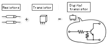
Digital transistors are covered by one of ROHM’s exclusive patents.
The first transistors with built-in resistors were developed by ROHM, who was awarded the patent rights. Digital transistors are also covered by one of ROHM’s exclusive patents.
How Does a Transistor Work?
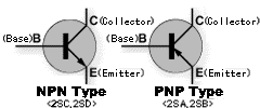
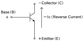
One analogy that helps explain how a transistor operates is to think of it like a water tap. In this case, electrical current works like water. A transistor has three pins: the base, the collector, and the emitter. The base works like the tap handle, the collector is like the pipe that feeds into the tap, and the emitter is like the opening where water pours out. By turning the tap handle with a small amount of force, we can control a powerful flow of water. This water flows through the pipe and out of the opening. Turning the tap handle slightly can dramatically increase the rate that water flows. If closed completely, no water will flow. If opened completely, water will gush out as fast as possible!
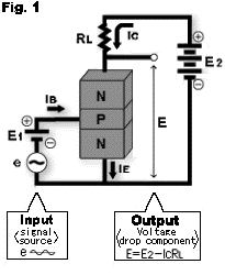
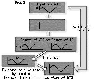
Now we can dive into a proper explanation using the diagrams below. A transistor has three pins, the emitter (E), the collector ( C ), and the base (B). The base controls the current from the collector to the emitter. The current that flows from the collector to the emitter is proportional to the base current. The emitter current, or base current = hFE. The setup shown uses a collector resistor (RI). If a current of Ic flows through RI, a voltage across that resistor will be formed, which is equal to the product of Ic x RI. This means that the voltage across the transistor equals: E2 – (RI x Ic). Ic is approximately Ie, so if IE = hFE x IB, then Ic also equals hFE x IB. Therefore, through substitution, voltage across transistors (E) = E2 (RI x le x hFE). Essentially, the input voltage E appears at the output after being converted into a voltage of IcRL.
(*1) hfe: DC Current amplification factor of the transistor.
Outline of a Transistor
Classification
Classified according to the shape.
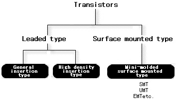
The size and shape of the transistor are determined by the power consumption and method of mounting. Broadly, transistors can be classified into leaded type and surface mounted type.
Typical Shapes of Transistors
(The figures show the cross-sectional views)
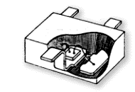
Mini-molded surface mounted type transistor
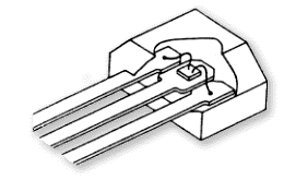
Insertion type transistor
Classification According to Construction
Transistors typically fall into two main types depending on their construction. These two types are bipolar junction transistors (BJT) and Field Effect Transistors (FET).
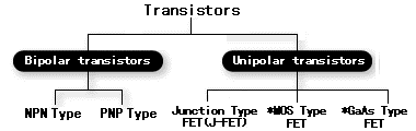
Bipolar Transistors
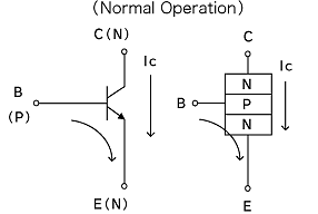
The word “bipolar” consists of two root words. Bi (meaning “two”), and polar (meaning “opposites”). A bipolar transistor is one in which the current through the transistor is carried by holes (positive polarity) and electrons (negative polarity). Bipolar junction transistors were the first type of transistor to be mass-produced in 1947 in the form of the point contact transistor (Bell Labs). They are a combination of two junction diodes, and are formed from either a thin layer of p-type semiconductor sandwiched between two n-type semiconductors (an n–p–n transistor), or a thin layer of n-type semiconductor sandwiched between two p-type semiconductors (a p–n–p transistor).
FETs
FETs (Field Effect Transistors) can generally be classified into three different types; junction type FETs, MOS (Metal-Oxide-Semiconductor) type FETs, and MES (Metal-Semiconductor) type FETs. Junction type FETs are mostly used in analog circuits such as those in audio equipment, and MOS type FETs are used mostly in digital ICs such as those used in microcomputers. MES type FETs are used for amplification of microwaves such as use in satellite broadcasting transceivers.
Classification According to Permissible Power
There are two broad classifications of transistors according to their permissible power: small-signal transistors and power transistors. These classifications are based primarily on the maximum rating of the collector power dissipation Pc.

Small-Signal Transistors
These are transistors whose maximum collector current (IC(max)) is about 500mA or less and the maximum collector power dissipation (Pc(max)) is less than 1W. These transistors are called small-signal transistors to distinguish them from power transistors and have the feature that they are generally of the epoxy molded type.
Power Transistors
If a transistor has a Pc of 1W or more, it is commonly classified as a power transistor. Compared to small-signal transistors, power transistors have a larger maximum collector current, maximum collector power dissipation, and also have a larger size to meet the heat dissipation. They are generally shielded by metal or have a structure with heat radiating fins.
In Japan, a transistor is called a “stone”. The word transistor is a combination of Transfer and resistor. Since a transistor is made of silicon which is the major element in all the rocks and stones on earth, many Japanese designers refer to a transistor as a stone.
Classification According to the Type of Integration
Apart from discrete type transistors, ROHM is also manufacturing composite transistors. These integrate several transistors together in order to meet various users needs. These include digital transistors with built-in resistors, transistor arrays consisting of multiple transistors in one package, and transistor units with simple circuits built into them.

Discrete Transistors
These are individually packaged transistors. They are becoming less common as the vast majority of transistors are now produced in integrated circuits along with diodes, resistors, capacitors and other electronic components, to produce complete electronic circuits.
Composite Transistors
A composite transistor (sometimes known as Darlington transistor) is a combination of two or more transistors (typically bipolar junction transistors) with the purpose of increasing the current gain.
*Digital Transistors
A digital transistor is a bipolar transistor with built-in resistors. These are the standard transistors that are used in circuit design.
Transistor Understanding Transistors
Reverse Current When ON
In an NPN transistor, the Base is at a positive bias, the Collector at a negative bias, and reverse current flows from the Emitter to the Collector. Also, please consider problems that may arise from usage as transistors (such as smaller current gain).
1.It has been determined that no problems, such as degradation or destruction, will arise from use.
2.In the case of an NPN transistor, B is symmetrical with C, and E with N. Therefore, C and E can be used as a transistor, even when connected in reverse. In this case current will flow from E to C.
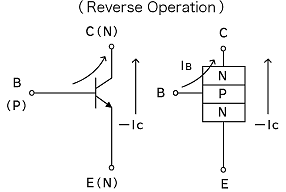
3.The following are characteristics of transistors connected in reverse.
- Low hFE (approx. 10% of the value of the forward direction)
- Low voltage resistance (around 7-8V, about the same as VEBO) The voltage may even be lower (below 5V) in some standard transistors (Please consider that excessively low voltage resistance may result in breakdown and degradation of characteristics)
- VCE(sat) and VBE(ON) should not change much
Package Power Permissible Loss
Package power permissible loss is when voltage is supplied to a transistor and the device begins to generate heat due to power loss due to current flow, particularly when the junction temperature Tj reaches the absolute maximum value (150ºC).
Calculation Method (Where △Tx is the amount of temperature rise when power Px is supplied)
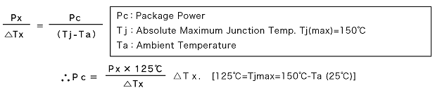
In this case, Pc, Ta, △Tx, and Px can be directly derived from measurement results. Tj is the only value that cannot be directly derived. Therefore, the following shows how to measure VBE, from which we can determine the junction temperature Tj.
In silicon based transistors, VBE will vary based on the temperature.
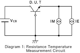
Therefore, the junction temperature can be inferred by measuring VBE. From the measurement circuit shown in Diagram 1, the package power Pc(max) condition is applied to the transistor (In the case of a 1W transistor, the conditions for supply are VCB=10VIE=100mA).
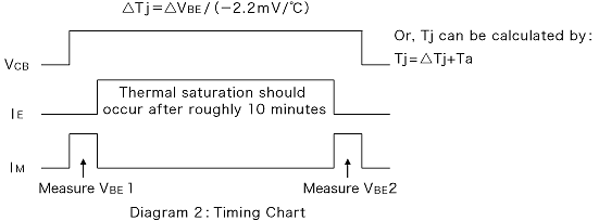
As seen in Diagram 2:
- VBE1 is measured as the initial value of VBE
- When power is supplied to the transistor, heat saturation will occur at the junction
- he value of VBE after will be VBE2
From these results: △VBE=VBE2-VBE1
Here, a silicon transistor will have a fixed temperature coefficient which is approximately -2.2mV/ºC. (NoteL Darlington transistors are due to the use of two transistors -4.4mV/ºC). Therefore, △VBE from the supplied power can be derived from the rise in junction temperature using the following formula.
fT: Gain Bandwidth, Cutoff Frequency
fT: Gain bandwidth indicates the maximum operating frequency of the transistor. At this time the collector current ratio with the base current is limited to 1 (hFE=1).
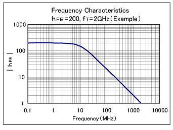
As the frequency of the signal input applied to the base approaches the operating frequency, the hFE begins to reduce. When hFE becomes 1, the operating frequency fT is referred to as the gain bandwidth. fT signifies the operating frequency limit. However, in actuality for operation the value will be about 1/5th to 1/10th that of fT.
f: Depends on the measurement equipment. Reference frequency for measurement.
VCE: optional setting – standard value is normally used for ROHM products.
Ic: optional setting – standard value is normally used for ROHM products.
